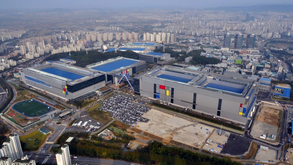
Amid tightening memory supply, production cuts for NAND MLC have become a clear trend among major memory makers. However, Samsung’s 2D NAND era may end sooner than expected. According to The Elec, the company could halt 2D NAND production at Line 12 in Hwaseong as early as March and convert the facility into an end fab for 1C DRAM to ease manufacturing bottlenecks.
The Elec reported that the line currently produces around 80,000 to 100,000 12 inch wafers per month and will be reassigned to late stage DRAM processes, including metal wiring steps. Samsung had already informed customers of the planned shutdown last year.
This move effectively marks the official close of Samsung’s 2D NAND chapter. The company began mass producing 1Gb NAND flash in 2002 and made a major breakthrough in 2013 with volume production of 3D V NAND. About 13 years after shipping its first batch of 3D NAND, Samsung is now set to shut down its last remaining 2D NAND facility.
Xi’an fab to play a larger role as Korea cuts NAND output
According to reports, the NAND capacity reduced in Korea will be offset by Samsung’s Xi’an plant in China, where production lines are being upgraded to newer generation 3D NAND processes.
Earlier, Global Economic reported that the Xi’an fab, which accounts for roughly 40 percent of Samsung’s total NAND output, is rapidly transitioning from 128 layer products, the 6th generation, to 200 layer and above, including V8, the 8th generation.
Samsung and SK hynix accelerate 1C DRAM investment
The conversion aligns with Samsung’s broader memory strategy, as 1C DRAM serves not only as the foundation for next generation HBM4 but also supports mainstream server products.
The Elec noted that Samsung is increasing 1C DRAM investment at its Pyeongtaek and Hwaseong sites. The P4 plant in Pyeongtaek was initially designed as a hybrid fab for DRAM, NAND, and foundry operations, but recent plans indicate it will be fully dedicated to DRAM. Older lines in Hwaseong are also being upgraded to the 1C DRAM process.
Rival SK hynix is also accelerating its 1C DRAM expansion. According to The Elec, SK hynix aims to reach 170,000 to 200,000 wafers per month for 1C DRAM alone, a sharp increase from the original plan of 90,000 wafers per month announced in April last year.
In addition, SK hynix is upgrading its M16 fab, converting the 1a DRAM line to 1C next year, with the 1b line to follow during the same period.
In this context, on February 25, SK hynix announced it will invest approximately KRW 21.6 trillion, about USD 15 billion, into its first plant at the Yongin Semiconductor Cluster before December 2030, bringing total investment in the facility to around KRW 31 trillion, or USD 21.5 billion.
