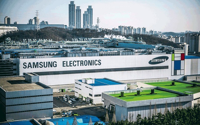
Samsung Electronics is stepping up its efforts in next-generation semiconductor technology, signaling a more aggressive push into leading-edge nodes. According to Hankyung, Samsung’s foundry division is now aiming to introduce a 1nm process by 2030, while simultaneously expanding its 2nm portfolio to attract major customers.
At the 1nm level, Samsung is expected to introduce new architectural innovations, including forksheet transistor structures. Up to the 2nm node, the company has relied on gate-all-around (GAA) technology, which improves power efficiency by enabling current to flow across all four sides of the channel. Forksheet builds on this by inserting insulating barriers between transistors, allowing tighter spacing and increasing transistor density within the same chip area.
Notably, TSMC is also expected to adopt forksheet structures for its own 1nm node beyond 2030. With a clearer roadmap in place, Samsung appears to be positioning itself to compete more directly with TSMC at the most advanced technology levels.
At the same time, Samsung is making significant progress at 2nm. Sources indicate that yields have now exceeded 60% at the upper range, reflecting meaningful improvements in production efficiency and raising expectations that its foundry business could return to profitability in the near term.
For Tesla’s 2nm AI chip, known as “AI6,” Samsung is developing a customized process called SF2T, with mass production planned for 2027 at its new Taylor, Texas facility. The company is also accelerating additional 2nm variants, including SF2P, expected to be used for next-generation smartphone application processors starting in 2026, and SF2P+, which is scheduled to follow in 2027.
Global Foundries Intensify the Race Toward 1nm
Beyond Samsung, other major players are also advancing their 1nm ambitions. According to Nikkei XTech, Rapidus aims to narrow its technology gap with TSMC to roughly six months at the 1nm node. The company is also planning to begin development of 1.4nm technology in 2026, targeting mass production around 2029.
Meanwhile, Economic Daily News reports that TSMC may move faster on 1.4nm, with initial trial production at its Central Taiwan Science Park facility expected by late 2027, followed by mass production in the second half of 2028.
As the industry pushes toward sub-2nm technologies, competition is no longer just about scaling, but about execution speed, yield maturity, and ecosystem readiness.
