Samsung has officially begun shipping commercial HBM4, marking a significant milestone in the race for high bandwidth memory tailored for AI and data centers. Built on the advanced 1c DRAM process and a 4nm base logic die, the new HBM4 generation not only raises the performance ceiling but also delivers major improvements in energy efficiency and reliability for large scale computing systems.
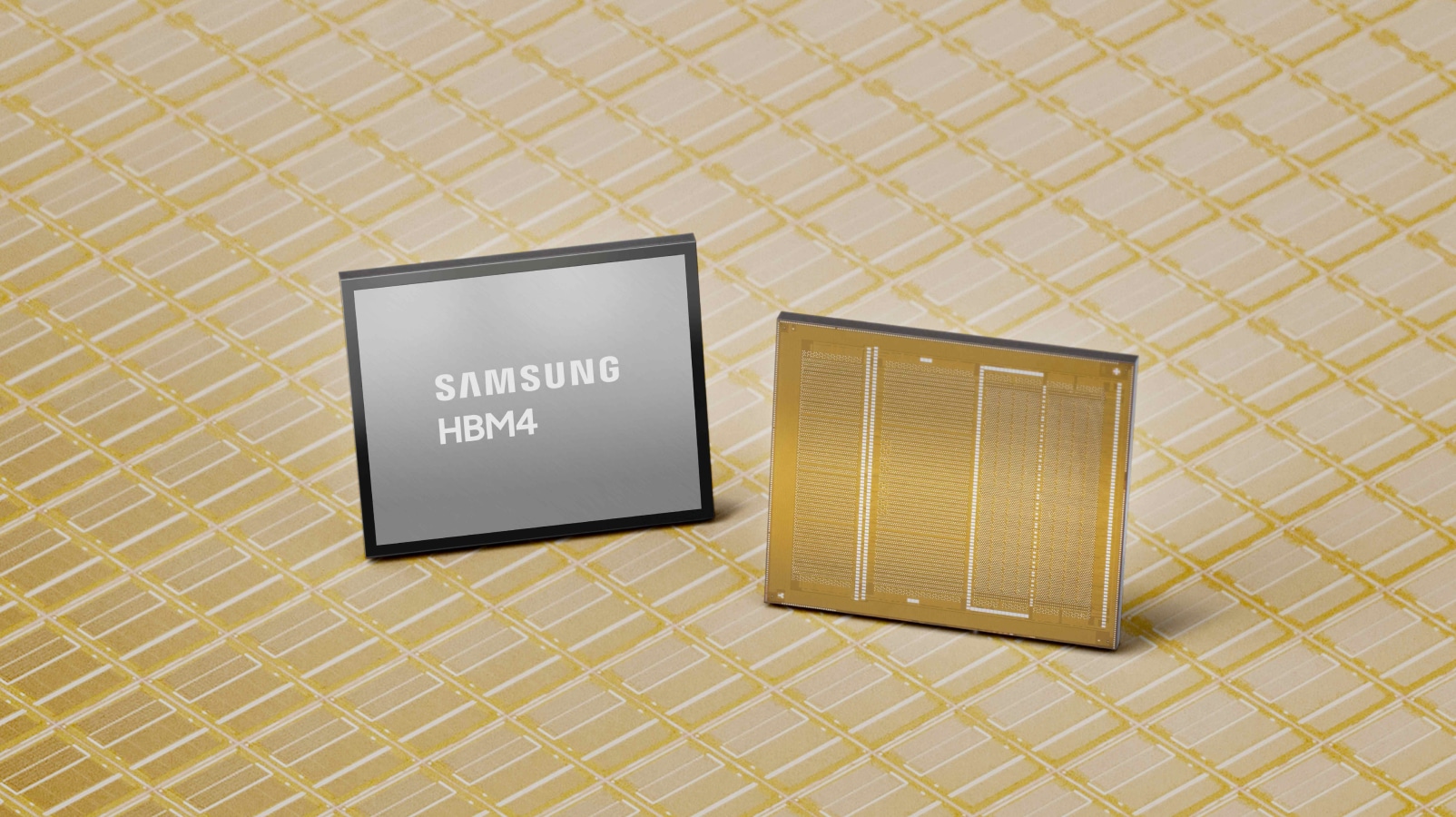
Samsung Electronics announced that it has started mass production of HBM4 and delivered its first commercial batch to customers, becoming the first company to bring HBM4 to market. This milestone positions Samsung with an early advantage in the next generation AI memory segment.
From the outset of mass production, Samsung achieved stable yields by applying its 6th generation 10nm class 1c DRAM process without redesigning the architecture. At the same time, integrating a 4nm base logic die optimizes performance, power consumption, and operational durability in parallel.
Samsung’s HBM4 delivers a stable data transfer rate of 11.7Gbps, approximately 46 percent higher than the widely used 8Gbps standard. It is also 1.22 times faster than HBM3E at 9.6Gbps and can scale up to 13Gbps when required, significantly reducing data bottlenecks in increasingly large AI models.
Bandwidth per stack has increased substantially, reaching up to 3.3TB/s, 2.7 times higher than the previous generation. With 12 layer stacking technology, HBM4 is offered in 24GB and 36GB capacities. A 16 layer version delivering up to 48GB is planned to support the roadmap of next generation GPUs and AI ASICs.
To address the challenge of doubling I/O pins from 1,024 to 2,048, Samsung introduced multiple enhancements in the core die to optimize power efficiency. By applying low voltage TSV technology and optimizing the power distribution network, HBM4 improves energy efficiency by 40 percent, enhances thermal tolerance by 10 percent, and increases heat dissipation performance by 30 percent compared to HBM3E.
Close integration between Samsung’s Foundry and Memory divisions through co optimization of design and process technology enables high quality and superior yield rates. Advanced in house packaging capabilities further shorten production and delivery timelines.
In parallel, Samsung is expanding technical collaboration with global GPU manufacturers and hyperscalers developing next generation ASICs. The company expects HBM revenue in 2026 to more than triple compared to 2025 and is proactively increasing HBM4 capacity to meet accelerating demand.
Following HBM4, Samsung plans to begin supplying HBM4E samples in the second half of 2026 and roll out customized HBM solutions from 2027 onward based on specific customer configurations, reinforcing its long term roadmap for high bandwidth memory leadership.
