ASML has reportedly achieved a major breakthrough in extreme ultraviolet (EUV) lithography technology by increasing light source power to 1,000 watts, a significant jump from the current 600-watt level. According to Reuters, this advancement could help raise chip output by as much as 50% by the end of the decade, as global demand for AI, high-performance computing (HPC), and data centers continues to surge.
Throughput Target: From 220 to 330 Wafers per Hour
Teun van Gogh, Executive Vice President responsible for the NXE system line, said the company aims to increase processing productivity from around 220 wafers per hour today to approximately 330 wafers per hour per machine by 2030.
Higher throughput means more chips produced within the same timeframe. More importantly, it directly reduces cost per chip - an increasingly critical factor as semiconductor process nodes become more complex and capital-intensive.
The 1,000W EUV Light Source at the Core
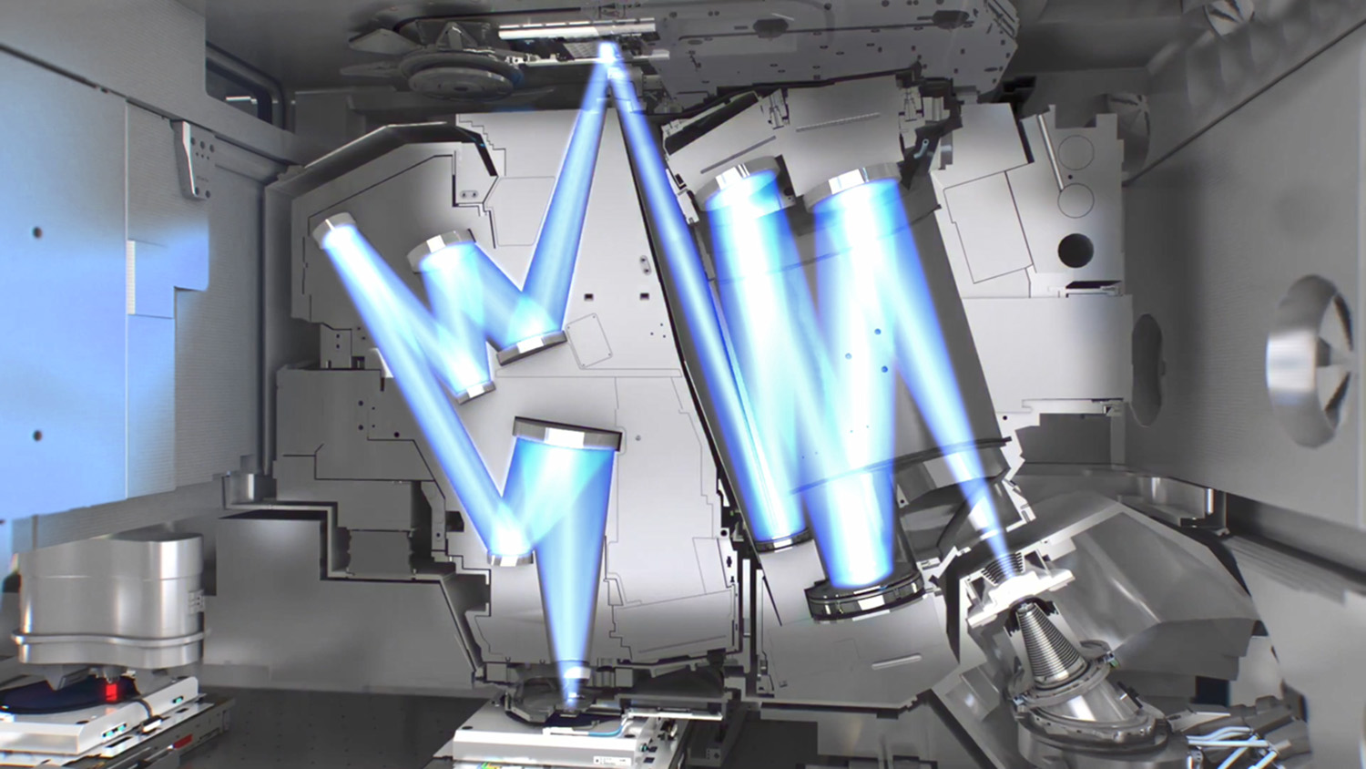
At the heart of this leap is the optimization of the EUV light source, widely regarded as the most technically challenging component of the entire system.
To reach the 1,000W milestone, engineers doubled the number of tin droplets fired per second to roughly 100,000. Instead of using a single shaping laser pulse as before, the new system deploys two smaller laser pulses, enabling more efficient conversion of tin droplets into plasma.
Inside ASML’s EUV machines, molten tin droplets are injected into a vacuum chamber and struck by a high-powered CO₂ laser. The resulting plasma reaches temperatures exceeding that of the Sun’s surface, generating light at a wavelength of 13.5 nanometers, the level required to pattern ultra-fine transistor structures.
This light is then collected and directed by ultra-precise optics supplied by Carl Zeiss AG, before being reflected onto wafers coated with photoresist. As light power increases, exposure time shortens, allowing more wafers to be processed per hour and significantly boosting overall output.
Integration Challenges in Existing Fabs
Despite the power breakthrough, the next challenge lies in deploying the 1,000W light source across existing semiconductor fabs.
According to Wccftech, ASML offers “Productivity Enhancement Packages” that enable customers to upgrade systems without replacing entire machines. However, thermal limitations in older NXE:3400C and NXE:3400D models suggest that not all platforms can easily support higher power levels.
As a result, rollout efforts are likely to focus on current NXE:3800E systems as well as next-generation High NA platforms such as the EXE:5000 and EXE:5200.
Reinforcing Leadership Amid Rising Competition
ASML views the 1,000W milestone as just the beginning of deeper performance improvements in the years ahead. However, the competitive landscape is intensifying.
Reuters reports that two U.S. startups, Substrate and xLight, have raised hundreds of millions of dollars to develop alternative EUV-related technologies.
In an increasingly fierce technology race, significantly boosting the power of the EUV light source - the core of the system is seen as a strategic move. It strengthens ASML’s technological lead and reinforces its pivotal role in the global semiconductor supply chain through 2030 and beyond.
