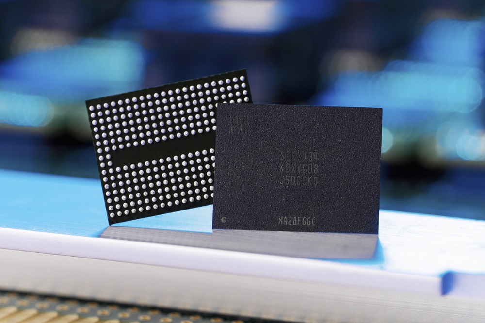
As the semiconductor industry searches for the next breakthrough in storage technology, Samsung and NVIDIA are expanding their collaboration into future memory research. Together with researchers from Georgia Tech, the two companies have introduced an AI model designed to significantly accelerate the analysis and development of ferroelectric NAND, a technology expected to pave the way for 1,000-layer NAND.
According to Sedaily, the PINO (Physics-Informed Neural Operator) AI model can analyze the performance of ferroelectric NAND 10,000 times faster than traditional simulation methods. This capability could dramatically shorten the time required for research and optimization of next-generation memory architectures.
Ferroelectric NAND: A promising memory technology for the AI era
Ferroelectric NAND is emerging as a potential breakthrough for the memory industry, with the ability to scale up to 1,000 stacked layers while reducing power consumption by as much as 96% compared with current technologies. This advantage is particularly significant as demand for storage capacity and energy efficiency continues to rise alongside the rapid expansion of AI infrastructure.
Unlike conventional silicon-based memory, ferroelectric materials can maintain a polarized state without requiring high external voltage. This allows electrons to move between positive and negative poles to store binary data (0s and 1s) while consuming far less energy.
The technology’s potential has prompted Samsung to ramp up related research efforts. According to intellectual property data cited by Sedaily, Samsung currently holds 27.8% of global patents related to ferroelectric technology, placing it ahead of competitors such as Intel, TSMC, and SK hynix.
AI drastically shortens memory R&D cycles
One of the biggest challenges in developing ferroelectric NAND lies in analyzing complex material properties and optimizing chip structures. In the semiconductor industry, TCAD simulations commonly used for this process can take around 60 hours per run.
With the new AI model, that process can be reduced to under 10 seconds, enabling researchers to test and refine designs far more quickly.
Toward 1,000-layer NAND by 2030
Currently, Samsung’s NAND technology reaches around 200–300 stacked layers. Ferroelectric technology is seen as a key pathway to scaling memory density further.
According to The Bell, Samsung is targeting 1,000-layer NAND around 2030 and recently unveiled the architecture for this next-generation technology at the International Solid-State Circuits Conference (ISSCC) in late February.
The design is considered an upgraded version of Bonding Vertical (BV) NAND, stacking four wafers, two cell wafers and two peripheral wafers to overcome structural limitations. Meanwhile, Kioxia is reportedly pursuing a similar approach under the technology name Multi-Stack CBA (CMOS directly Bonded to Array).
